This article is part 1-B (see part 1, then part 2, part 3) in a series were we try to build a MIDI instrument from a bunch of SN76489s, which is the sound chip used in the Sega Game Gear, the BBC Micro, the Neo Geo Pocket and quite a few others.
If you’ve read the previous installment, you may have noticed this little aggregation of curious things:
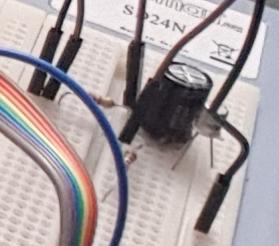
That’s an amplifier, that’s what! Although a pretty bad one. In this article we’ll dive into the design I used here, and start exploring the fascinating, daunting, seemingly-infinite territory of how transistors work.
Note before we start: I’m really out of my depth here, and just trying to have fun. I’ve completely forgotten the little formal training I might have ever had in electronics. I don’t know what I’m talking about, so don’t quote me on anything. You have been warned.
Why an amplifier
The SN76489 chip can output up to 10 mA, which while enough to drive a small load for test purposes, begs for some amplification. Moreover, a few components I had bought or salvaged1 a while ago were looking at me with begging eyes, so this provided a good excuse to indulge and build an amplifier. However, we only need it for testing and we’ll drop it pretty soon: it does not have to be perfect, and only has to drive my little speaker.
This article will actually be a bit of a time warp: at the time when I actually build the amplifier, I did not have any measurement tools so I couldn’t validate nor understand what this was really doing. This was a bit frustrating. Since then though, I bought a little EspoTek Labrador, so we can now take on the challenge.
Quick & dirty design
I settled on the simplest-looking2 amplifier design I could get my hands on3, which you can see below. It’s pretty bad (for multiple reasons), and will damage your speaker if left on for too long. Thankfully this is only for testing, so that’s OK. It looks like this:
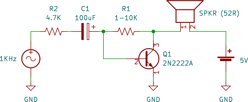
What do we have here? From left to right:
- A signal source. We’ll simulate our TI chip here as a 1 KHz sine4 wave signal.
R2: a current-limiting resistor to simulate the limited current.C1: coupling capacitor.R1: resistor for biasing the transistor. Its exact value isn’t too clear, some use 2 KΩ. We’ll talk about that.Q1: transistor to provide the amplification.SPKR: either a speaker or a funny hat, you decide. Most speakers are about 4 Ω or 8 Ω, but not mine, no sir. 52 Ω for you.- And to the right, our voltage source to feed the amplification. It’s only 5 V so I can power it from the Arduino.
Input stage
Let’s look at the input stage first:
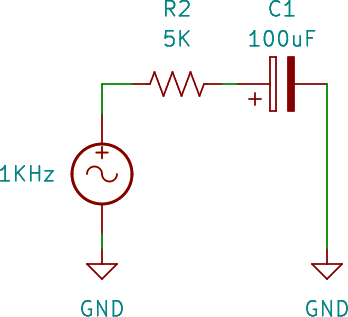
I configured the signal generator to output a 2 V amplitude sinewave. Combined with the 5 KΩ resistor, we get a current amplitude of 0.4 mA. That’s small, but since the usual factor for current amplification is around 100, we get a maximum amplitude of 40 mA.
However, just as is the case with the TI chip, the generated signal is not centered on zero but always positive. To remove that positive bias and get a nice AC signal, we must use a coupling capacitor. Now, while this is again super common stuff, I found that notion interesting enough to warrant its own measurement:
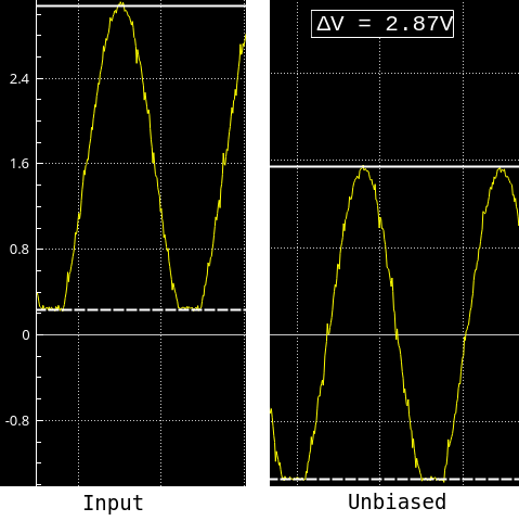
On the left is the signal voltage, while on the right we have the voltage at the terminals of R2. The signal looks cut at the bottom, but I think that’s an artifact of my signal generator, or of my setup here.
Note that even without this DC bias from the input source, the coupling capacitor would have been required anyway to block the bias we’ll apply on the transistor’s base.
A word about transistors
Throughout this article, we’ll focus on NPN BJT transistors and ignore the other categories.
An transistor allows a certain current through its collector based on the current flowing through its base (both flow to the emitter). Note I’m talking about current only: this is probably more complicated than that, but transistors are inherently current devices. I found it easier to reason about current first, and introduce voltage only where necessary.
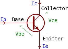
You get , which is why you can amplify a signal: small signal in input, bigger signal in output, mostly constant factor between the two.
There is a minimum for the transistor to turn on. When this threshold is reached, is at its maximum (≅0.7 V) and mostly stays there, and the transistor starts allowing current through the collector. In a real circuit, this will result in variations of , to respect the above relationship between & . However, the transistor only allows current through the collector, it does not create current: if not enough can be provided by whatever source is connected to the collector, reaches a minimum (≅0.3 V) — this condition is called saturation.
It must be noted that varies a lot with operating conditions (, temperature, etc.) and with transistors (even within the same model you get different values). It seems common to assume a value of 100, at least for a start. It can easily vary between 50 and 300, so good circuits are designed as to not depend on the exact value too much.
Biasing the transistor’s base
We want to amplify a signal that varies between -1 V and 1 V. When amplifying a signal we must bias the base of the transistor up (meaning, apply a DC voltage) for two reasons:
- First a transistor only works one way, so AC signals are a no-go — we must get a positive signal only. Thanks to our coupling capacitor
C1, applying a voltage will not alter the signal: it simply moves it up, exactly how we moved it around 0 in the section above. - Second, even if our signal is 0-2 V, our transistor will constantly turn off when reaching 0 V and then back on — this would heavily distort the signal. Hence, we want to positively bias the transistor so our lower input value will still keep the transistor on.
This is the reason we have R1, to force a DC voltage at the base. The input signal will then pull or push current at this same point, influencing , which in turn will influence . Magic!
This is also one of the reason why this particular amplifier design is bad: when on, even without signal, we’ll always have some current running through our speaker. Better designs work around that issue with a different placement of the speaker allowing the use of another coupling capacitor.
Initial current values
We will talk in more details about the exact value and effect of R1 in a section below, because it is a treat. Notably, I’ve seen a value of 2 KΩ used here and there, but at this point we have no idea why.
What we do know is that a value too great will not let enough current through to turn the transistor on. So for a start, let’s choose a big value as a potential maximum and calculate its current in the circuit in normal operation mode, if only to check that there is enough to turn the transistor on in the first place.
Let’s start simple: while the transistor is off, no current flows through the collector so we have both and .
In turn, the base current is . The lowest current we can get at the base while the transistor stays off is when approaches 0.7 V.
We have . Let’s take a big as a starting point. This also makes above small enough to ignore.
We get: . This is above which the 2N2222A’s datasheet seems to imply as the minimum base current, so we’re good: we can turn the transistor on.
Operating current values
But wait! Now that current is flowing through the collector, a significant portion of is diverted away from the base, and the whole situation has changed. So the above calculation, while a nice way to get us warmed up, is just not valid — at least not while operating the transistor.
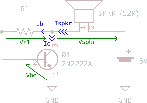
Let’s start again with this new condition and see if we can solve it easily:
We’re trying to determine , and we know and some of the resistances so let’s start from there and make pop in every non-constant:
Which gives us now:
Hurray! That’s still above with a nice margin.
Before we move on, let’s get a feeling of what the above equation for implies:
- The lower the resistance , the greater the base current.
- Similarly, the lower the resistance , the greater the current in the circuit, so the greater the base current.
- Interestingly, the greater the , the more diverted current into the collector, so the lower the base current.
In operation without signal
Now that we have our circuit and sort-of understand how this is supposed to work, let’s build it and start measuring. As opposed to the above section, let’s start with a small because at this point, I figure the lower the bias resistor, the greater the base current, the better (spoiler alert: this is wrong).
Will we get the expected results according to the equation above?
Well, close but not exactly.
First measurements
Confounded by the early results, I decided to do measurements with 2 values. Here are the results:
Wow, OK, our assumption of was way off. And this factor does indeed vary a lot. However, if we use the corrected value in the equations above, we do get the correct relationship between and so at least we’re good here.
However something really strange happened: when testing both circuit, I got a clearly stronger amplification with the biggest . Why is this?
We see in the table that looks higher with a greater resistance. Could this be the reason (Spoiler alert: nope)? And if so, what is the biggest value we can get?
Exploring Beta
I got all worked up about this thing, so let’s measure it on our transistor.
It’s not too hard to do: with the signal generator, I can create a voltage sweep from 0 V up, and through a fixed resistor create a known . Then, supplying a small load at the Collector with a fixed voltage, I can measure the resulting voltage drop across the load and deduce .
This looks like this:
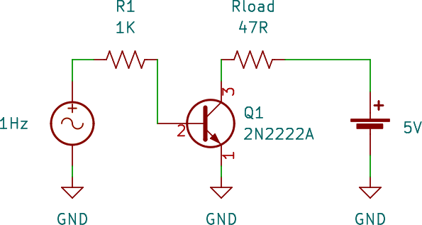
Or like this on my breadboard with a nut for, ah, scale:
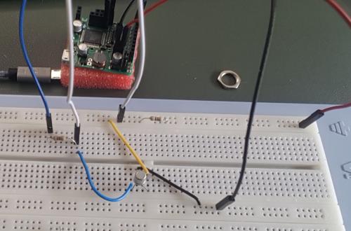
Note I dropped the speaker for an actual resistor: the speaker was causing too much noise when the transistor suddenly turned on.
Out of this, we get the following voltage measurements:
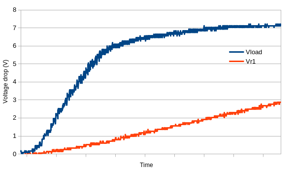
You can’t see it too well, but starts with a plateau, were most of the voltage drop is (I guess) eaten up by the base’s diode, and very little current is passing through. Then, we get a nice linear-ish relationship, until we approach saturation and plateaus again.
What we really want to observe are the currents and resulting values. However the measurements are very noisy: the Espotek’s resolution isn’t too great5, so we need to average the heck out of this:
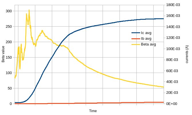
We get similar-looking current curves, and a beta approximation. Again, the spikes at the beginning are probably due to the measurement resolution, which is not sufficient at the start of the graph even when averaged. The low resolution really hurts when the values are small.
While the exact values are not too exploitable, this tells me a great deal about this parameter:
- It does vary, especially (as expected) when nearing saturation.
- A value between 150 and 250 is to be expected at low currents, although huge variations are indistinguishable from measurement errors.
- It seems to drop a little when the base current gets higher, before saturation — although again it’s hard to tell if it’s just the error factor getting lower.
However, this does not tell much about the difference in sound output relative to . I suspect the variations we were observing previously are measurement errors that don’t explain the significant difference in power output I was hearing.
We need more measurements while the thing is operating.
In operation with signal
Let’s measure the influence of the input signal on the output, and try to understand it.
Initial assumptions
Let’s be naive for a moment. If we consider the current amplitude of the input signal applied to the base, the amplitude of the output should be relative to , right? We apply a amplitude to a resistance: we expect of current amplitude in the output.
To actually measure the output signal, we’ll measure the voltage drop across multiple points, and get the bias & the amplitudes. We’ll repeat the operation with multiple values.
Here is a plot of the output currents. I also added their measured ranges, along with the naively expected ranges and a percentage of the former over the latter:
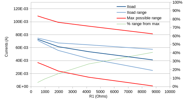
Note Iload is considered interchangeable with Ic for simplicity in this graph, but this does not change the results too much
This invalidates our naive calculation above, and confirms what I was hearing: while a lower values drives the mean current lower (as expected), the amplitude gets bigger so the sound is louder. Why is that?
Negative feedback
Well, poking around in the circuit, I finally got the answer. It turns out the approach above completely overlooks the fact that the transistors varies the voltage at the collector to regulate the current, which influences R1, and in the end its base current. Let’s see what it looks like:
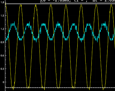
In the above image, we see the input signal vs. the collector voltage (from which the bias current is derived). Their phases are opposed, ain’t that a treat? The more current must get drawn into the collector, the lower must be, so less voltage drop is available for the biasing resistor. The bias goes against the signal, which dampens the effect of the latter. I guess that this is textbook negative feedback, and that it’s been painfully obvious for a while for the more electronic-savvy of our readers.
I may be completely off the mark with what’s about to follow, but let’s try to calculate all that. Let’s start from , dropping the assumption that it is equal to :
Let’s assume that so we can gain some clarity without losing too much precision :
This hints at the relationship we observed above: shrinks as grows, by a value inversely proportional to the resistance value.
Let’s now try to see the influence of the signal. At any point in time, we can express as a function of the current pushed (or pulled) by the input signal :
Which we can expand as:
Let’s rename the constants to make this readable:
Again, this confirms that the influence of over (and so over ) is relative to the value of — the greater the , the lesser the input signal is dampened (up to no dampening at all when reaches ), and the greater the output’s current amplitude.
Let’s plot that to compare against our previous measurements:
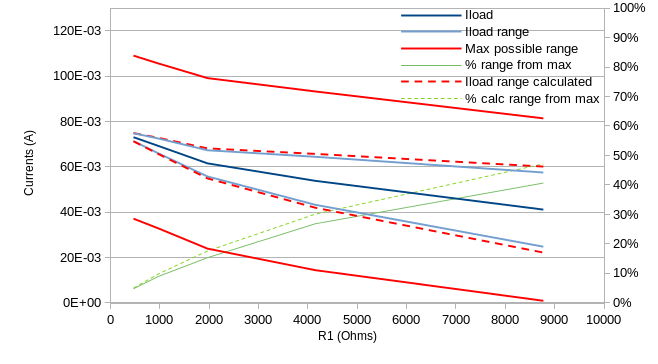
Not too far off! Again, I have no idea if the calculations above are anything correct but this is encouraging. I’ll consider that good enough for now.
In any case we understand why going with a greater helps: it limits the negative feedback that is dampening the signal’s influence on the output. Also, it reduces the constant current applied to the speaker which, while this whole thing is definitely a bad design anyway, helps a little.
Conclusion
And there we go! We started with a completely unknown amplification circuit diagram and managed not only to make it work, but understand and visualize the use of each of its components. We took a detour to measure the factor of our transistor. We also dug into the negative feedback applied to the transistor’s bias, and managed to find a calculation that reproduces our measurements.
Now this raises some questions:
- Why not connect
R1from the voltage source directly instead of at the collector? - Could we place the speaker somewhere else so it does not suffer from the constant DC voltage even without signal?
Well, I would guess that’s why an actual Class A amplifier looks the way it does. And no, I’m not going to build one, that’s a rabbit hole for another time. It’s time to go back to our project.
See you in part 2.
-
Salvaged from an oven circuit board that fried when I spilled milk on it, but life, huh, finds a way. For capacitors, at least. ↩
-
I would not necessarily make the very same choice now: simple-looking does not necessarily equate to easily understandable. ↩
-
There are good, simple amplifier designs to be found everywhere, along with tons of details & explanations. Notably, Electronics Tutorials is probably a source I’ll get back to in the future. However, as a complete neophyte, I found the Simply Put YouTube channel to provide a very approachable perspective when trying to form an intuitive understanding of what’s where and why. His Simple and Quick Audio Amplifier presents the design I copied here. ↩
-
I chose a sine signal instead of a square signal because this makes it much easier to visualize distortion and clipping in the output signal. ↩
-
As we can see in the documentation, there is a mode to get a 12-bit resolution using both inputs at the same time in the Multimeter mode, but I couldn’t manage to export a
csvfile to exploit the values, so I’m stuck 2 channels, 8 bits. I guess that’s kind of fitting for this project, though. ↩