A while back, I started playing with SN76489 chips1. I’ve always been a bit fascinated with chip music, old 8-bit era computers and electronics, but never seriously dabbed into any of these things. So what began as a playful experiment quickly started to scratch some pretty serious itches.
This series (see part 1-B, part 2, part 3) will be a sort of idealized recollection of what took place over the past 6 months or so, where I tried to make music with these things. Apologies for the relative lack of pictures — I did not think for a moment that I would actually go anywhere with this.
There is a lot to talk about, so this will be split up: in this part 1, we will concentrate on setting up communication with a common SN76489 chip and getting some sound out of it. In part 2, we will start playing notes and we will set up MIDI control of the various channels. In part 3, we stick multiple chips together, build a mixer circuit and a case for our contraption and add even more features to our synth to make some music with it.
Chip music?
I guess we should start here. My understanding of what is called chip music today is music made at least partly with a set of simple waveforms such as pulse waves (square waves), triangle waves, and noise channels. We can probably throw FM synthesis in the mix as well. This is a legacy from 8-bit-era video games & computer systems: the limited capacity of the machines required the use of programmable sound generators (to which the CPU sends notes). Moreover, the cost constraints meant using few, basic chips. As a result, you get simplistic sounds on very few parallel voices.
Here are a few examples2:
- 1942’s Main background music (BGM) — or rather ambience made with percussive elements:
- Clean Sweep’s Sound 1 for background sound effects:
- Donkey Kong’s Game start with some triangle wave bass to keep you on your toes:
These constraints, as is often the case, meant that talented people started to work around the limitations to get more and more juice out of these systems. A typical sound started to emerge, a kind of “scene” grew out of isolated silos, and you get gems everywhere you look. It’s fascinating.
- Silver Surfer’s BGM on NES — arpeggios, fast rhythms, tone sweeps, the works:
- Bomb Jack’s on Game Boy — different platform, different sound but similar principles:
Nowadays I guess this sound is 100% associated with old video games. However, chip music is still being made today, sometimes on real hardware3, sometimes more as a reference incorporated into more complex songs. Here are two examples of the former:
-
🎵 Chipzel - Focus on bandcamp — Super Hexagon’s soundtrack
-
🎵 Kommisar - The Maid and the Pocket Watch of Blood on bandcamp.
I just scratched the surface here, and I could not be thorough even if I tried anyway. Hopefully that’s enough to give an idea. If you want to know more about the old days of chip music and its creators on the Japanese side of things, I found the documentary Diggin’ in the Carts to be interesting and approachable.
The SN76489 chip
Let’s get back to business.
This TI chip and its variants were used in various computers & game systems from that era: from arcade games, to the BBC Micro, to the Sega Master System & Game Gear. It has 4 channels: 3 square wave & 1 noise. It it sounds similar to what we’ve listen to above, but even more limited: no sample playback, no triangle wave, 50 % duty cycle pulse wave only.
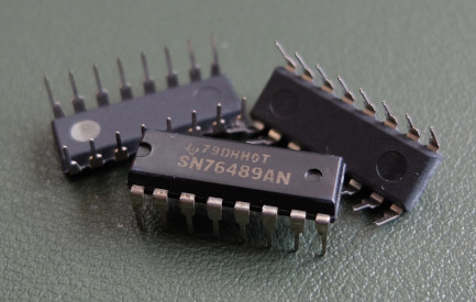
They are still pretty easy to find today, and on some rainy day I purchased a batch on eBay. I settled on the AN variant, which accepts a 4-MHz clock.
First stages of communication: sending bytes
We need to try to talk to this thing, so let’s take a look at the chip’s datasheet.
Pin layout
This is the chip’s layout:
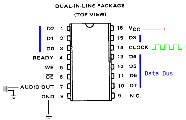
First, the data bus is made up of pins D0-D7. The chips needs an external clock signal, not only for operation but also as a way to derive the notes frequency — that’s on pin 14. The sound signal is then output on pin 7.
The remaining pins are used for synchronization:
CEon pin 6 (inverse logic): Chip Enable, unless pulled to ground the chip will ignore what’s happening on the data bus. It’s weirdly spelled OE in the above picture, but later referred to as CE.WEon pin 5 (inverse logic): Write Enable, to be pulled to ground when data is ready on the bus.READYon pin 4: high when the chip is done reading data.
The inverse logic thing means that the voltage you set is opposed to the logic: pull low for true, and high for false.
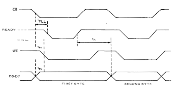
Ergo, sending a byte to the chip is a matter of:
- Setting
CEto true to select the chip (this can be wired to ground if there’s only one chip) - Putting our data byte on
D0toD7. - Setting
WEto true to indicate that data is ready. - Waiting for
READYto be true.
Vague memories from school 15 years ago tells me this is pretty standard stuff. So, time to get the Arduino out?
Data layout
Wait! What should we send?
The chip is controlled by setting its internal registers, which is done by talking a simple protocol on the data bus. There are 8 registers:
- 10-bit registers for channel 0-2’s frequency control.
- a 3-bit register for channel 3 noise type.
- 4-bit registers for each channel’s attenuation (volume).
In order to set a register value, the most significant bit (MSB) is set to 1, the 3 next bits select the register, and the rest is devoted to the register’s content. For the 10-bit registers, data is sent in two stages, and the MSB is set to 0 to indicate the second stage.
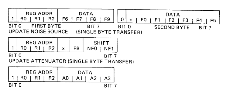
Note how D7 is the LSB and D0 the MSB, “big-endian” fashion.
Clock
We also need a clock signal for this whole thing to work. I don’t have a quartz around, and I sure don’t know how to make a proper clock circuit, so I looked for other options.
It turns out4 the Arduino’s SoC is quite flexible and you can use it to generate pretty fast signals with counters & interrupts. Let’s get a deeper look at the ATmega328P datasheet to see precisely what we can do.
The ATmega328P has multiple internal timers, with different resolutions and functionalities. They can be configured to trigger interrupts on delays, compare values, generate waves via PWM, at high frequencies (close to the SoC clock) while letting the CPU do something else. Timer 0 is used by regular Arduino functions such as delay, so we must leave it alone. However Timer 1 and 2 are up for grabs.
Timer 1 supports a mode called Clear Timer on Compare Match (CTC). When properly configured, we can get the following behavior:
- The timer increments a counter in
TCNT1at each clock cycle - When the value reaches a top value stored in
OCR1A:- The counter
TCNT1is set back to 0. - The timer event happens: in our case, we want the output pin
OC1Ato be toggled.
- The counter
The maximum output frequency can therefore be obtained by setting OCR1A (the top value) to 0: the output pin gets toggled at each clock cycle, so a full period takes 2 cycles. Hence, the maximum clock we can generate is 8 MHz on our 16 MHz SoC. In our case we want to generate a 4 MHz clock signal: we must set the top value OCR1A to 1 so the timer is reset every other clock cycle.
In the general case, the output signal’s frequency will be 5.
To configure this mode properly, according to the datasheet we need the following parameters:
WGM1 (4 bits) = 4 = 0b0100for CTC mode compared againstOCR1A5COM1A1 (1 bit) = 1for toggling the output on compare match5- Disable the interrupts that could be generated to the CPU5 — simply have the signal on the output pin.
CS1 (3 bits) = 1 = 0b001to disable the prescaler6 that can change the incrementing speed, but is too coarse for our use.
Those values are spread over multiple registers, so we must set bits individually:
TCCR1Astores COM1A1 and WGM1 bit 0 & 17,TCCR1Bstores CS1 and WGM1 bit 2 & 38,TIMSK1stores the various interrupt enable flags9.
In the end, we need something like the following code:
void setupClock()
{
    // Setup the clock to drive the SN76489
    pinMode(clockOutputPin, OUTPUT);

    // Set Timer 1 CTC mode with no prescaling.  OC1A toggles on compare match

    // WGM1 = 0100: CTC Mode against OCR1A
    // WGM1 bits 1 and 0 are in TCCR1A
    // WGM1 bit 2 and 3 are in TCCR1B

    // COM1A0 sets OC1A (arduino pin 9) to toggle on compare match
    TCCR1A = ( (1 << COM1A0));

    // Set Timer 1  No prescaling
    TCCR1B = ((1 << WGM12) | (1 << CS10));
    // Make sure Compare-match register A interrupt for timer1 is disabled
    TIMSK1 = 0;
    // Counter top value
    OCR1A = 0;
}
Testing setup
Finally, we can get the Arduino out.
Setting up a data bus on a breadboard is easy to get wrong, so at this stage we want to keep things simple to test our setup. We’ll simply set channel 3 to max volume, and then cycle between noise values 0 to 7 with a small delay in-between. This means we’ll send the following commands:
| Hex | MSB | Register | Value |
0xF0 |
0b1 |
0b111: Noise Attenuation |
0b0000: 0 (max volume) |
0xE0 |
0b1 |
0b110: Noise |
0b0000: Periodic, N/512 |
0xE1 |
0b1 |
0b110: Noise |
0b0001: Periodic, N/1024 |
0b1 |
[…] | ||
0xE7 |
0b1 |
0b110: Noise |
0b0111: White, Tone Generator #3 output |
0b1 |
Cycle back… |
Here is one picture I took of the setup in a flash of clarity of mind:
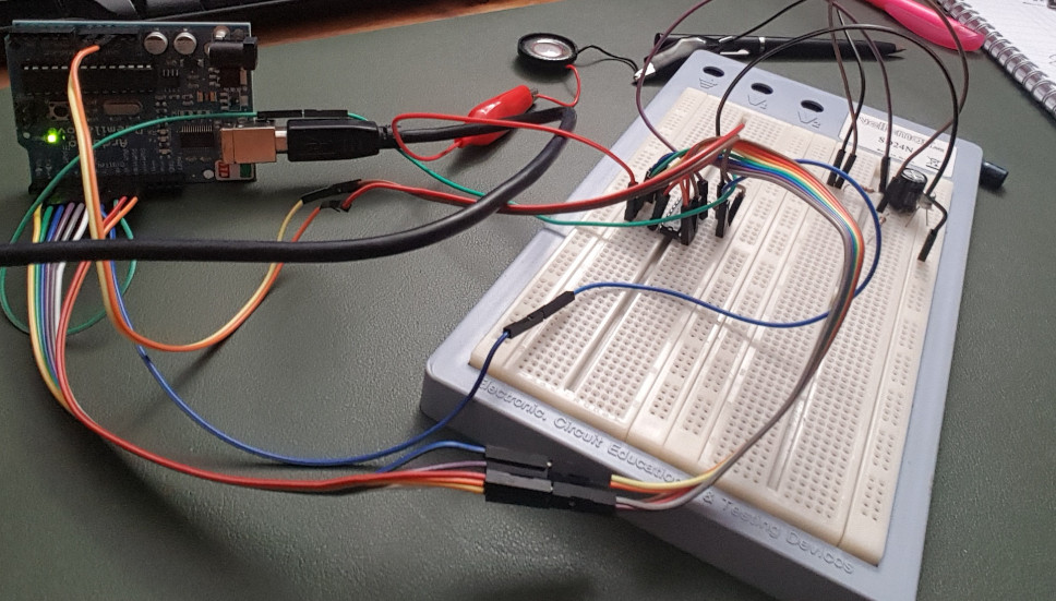
You can barely make out the pin layout, but it does not matter too much: there are enough pins on a simple Arduino to dedicate one to each chip’s pin. Note I decided to revert the big-endian-looking data bus into little endian on the Arduino side, because my brain is wired that way and the code looks simple to me:
void writeByte(byte value)
{
  for (int i=0; i < 8; ++i) {
    digitalWrite(DATA_BUS_PIN0 + i, (value >> i) & 1);
  }

  // [...] Wait for write enable
One trivial detail: I pulled CE to ground via a pull-down resistor. I think it was 4.7 KΩ? At 5 V, a value of ~5 K drains an acceptable ~1 mA, and this value seems to work well.
And finally, this is what is sounds like through the feeble speaker you see on the picture:
Our first milestone has been reached!
Mistakes were made
Now, don’t think for a minute that this went smoothly. It did not, and I did a fair share of rookie mistakes.
First, notice how pin 0 & 1 are not wired on the Arduino? That’s because pin 0 & 1 on the Arduino are dedicated to the serial transmission if you set it up (which I did, because logs). So of course, if you wire them up to the chip, you’re going to have a bad time. This is reflected in the actual writeByte code.
A second, big issue I had was with dealing with the READY signal. I could not, for the life of me, see it pull up! It was just… standing there, flapping in the breeze. I’m probably missing something trivial though. I may revisit this in the future, if I put a chip back on the breadboard. In any case, after a while I decided to cut my losses and ignore the signal, use a delay instead, and move on.
Next steps
We’d now be ready to make the chip play some simple tunes on one of the other channels, or do some cool sweep. In part 2, we’ll set up the MIDI side of things so we can control the board from a keyboard or a DAW, and improve from there.
But first, in part 1-B, we’ll dive into the little amplifier you can vaguely see on the picture above.
-
I’m certainly not the first one to do so! There are plenty of examples to be found:
- Fun with chips #2 by Steve Mansfield-Devine was certainly an inspiration to go through this first phase of the project.
- Weekend project by transitorykris.
- SN76489AN demo by James Dalton.
-
There are a few communities dedicated to extracting & preserving these artifacts in the form of, for example, VGM files. VGMRips is a good starting point. In this page, I reproduced short samples of mp3s you can listen to there, in the hope that it’s OK. ↩
-
The original GameBoy is especially appreciated for its versatility & textures, and got popular notably through LSDJ, a tracker made for the hardware. ↩
-
§15.9.2 Clear Timer on Compare Match (CTC) Mode page 100-101. ↩ ↩2 ↩3 ↩4
-
§16.1 Timer/Counter0 and Timer/Counter1 Prescalers: Internal Clock Source page 114. ↩